Interface protocols
I²C protocol
General remarks
For I²C only two bus lines are required: a serial data line (SDA) and a serial clock line (SCL). Both lines are connected to 5V via on-board pull-up resistors so that they are pulled high when the bus is free. The I²C interface of the Pozyx tag is compatible with the I²C Specification UM10204 Rev. 03 (19 June 2007), available at http://www.nxp.com. Pozyx supports I²C standard mode (100kbit/s) and fast mode (400kbit/s), only 7-bit address mode is supported. The Pozyx tag I²C interface uses clock stretching.
The default I²C (slave) address of the Pozyx tag is 1001011b (0x4B). The alternate address is 1001010b (0x4A). The alternate I²C address can be selected by soldering a 0Ohm resistor on the pads denoted by 'I2C LSB' on the back of the pozyx tag.
Register write operation
I²C write access can be used to write multiple data bytes in one sequence. The sequence is outlined below and can be seen in the figure below.
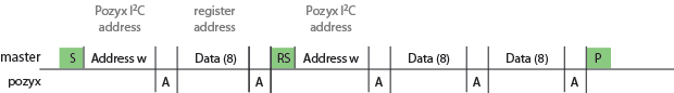
The sequence begins with the start condition generated by the master, followed by the 7 bits slave address and a write bit.
Pozyx acknowledges.
The master sends the one byte register address.
Pozyx acknolewdges.
The master generates a repeated start, followed by the 7 bits slave address and a write bit.
Pozyx acknowledges.
The master sends a data byte to be written at the register address.
Pozyx acknowledges and steps to the next register address.
The master may repeat step 7 or terminate transmission by generating a stop signal.
Register read operation
I²C read access can be used to read multiple data bytes in one sequence. The sequence is outlined below and can be seen in the figure below.
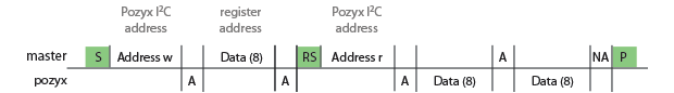
The sequence begins with the start condition generated by the master, followed by the 7 bits slave address and a write bit.
Pozyx acknowledges.
The master sends the one byte register address.
Pozyx acknowledges.
The master generates a repeated start, followed by the 7 bits slave address and a read bit.
Pozyx acknowledges.
Pozyx sends a data byte from register address, and steps to the next register address.
The master acknowledges and pozyx will repeat step 7. Or the master does not acknowledge, and generates a stop signal to terminate the transmission
Function call operation
I²C function call operation can be used to trigger a function on the pozyx device. The sequence is outlined below and can be seen in the figure below.
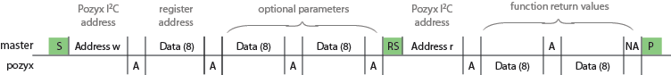
The sequence begins with the start condition generated by the master, followed by the 7 bits slave address and a write bit.
Pozyx acknowledges.
The master sends the one byte register address.
Pozyx acknowledges.
The master can (optionally) send a parameter byte.
Pozyx acknowledges.
The master may repeat step 5 or can generate a repeated start, followed by the 7 bits slave address and a read bit
Pozyx acknowledges.
Pozyx sends a data byte from register address, and steps to the next register address.
The master acknowledges and pozyx will repeat step 7. Or the master does not acknowledge, and generates a stop signal to terminate the transmission.
USB protocol
General remarks
Starting from firmware version v1.0 it is possible to communicate with the Pozyx device over USB. The pozyx device will emulate a virtual COM port that allows the user to connect with it through a serial port. The settings for this serial port are:
baudrate 115200
8 bits
no parity
1 stop bit
Register write operation
USB can be used to write multiple data bytes to a pozyx register. The command to write to a register looks as follows:
W,<Reg address>,<Data>with <Reg address> the register address in hex format (without leading 0x) to start writing, and <Data> a string of data in hex format (without leading 0x).
Example: the following command writes the data bytes 0x0A 0x12 0xBA starting at register 0x30:
W,30,0A12BAAfter the example write command, the register content will look as follows:
register | data |
|---|---|
0x30 | 0x0A |
0x31 | 0x12 |
0x32 | 0xBA |
Register read operation
USB can be used to read multiple data bytes in one sequence. The command to read from the registers looks as follows:
R,<Reg address>,<Num bytes>with <Reg address> the register address in hex format (without leading 0x) to start reading, and <Num bytes> the number of bytes to read (in decimal). The Pozyx device will respond as follows:
D,<Data>with <Data> a string of data in hex format (without leading 0x)
Example: the following example reads 3 bytes starting from the register address 0x00, which is the register:
R,00,3The pozyx device will respond something like this (the actual data may be different):
D,430123Function call operation
The command to perform a register function looks as follows:
F,<Reg address>,<Params>,<Num bytes>with <Reg address> the register address in hex format (without leading 0x) of the register function, <Params> a string of parameters in hex format (without leading 0x), and <Num bytes> the number of bytes that the function will return.
Example: the following example executes the register function at register address 0xA3 with parameters 0x0A 0x15 0x56. One return byte is expected.
R,03,0A1556,1